Debugging & UART
A serial port from a shift register and a counter, so the board can tell us what it is doing and listen to what we type.
In this article
What are we trying to do?
An FPGA design has no screen and no printf. When something goes wrong, the board just sits there. Before we build anything big, we want a way for the hardware to talk to the PC: send bytes that show up in a terminal, and receive the keys we press.
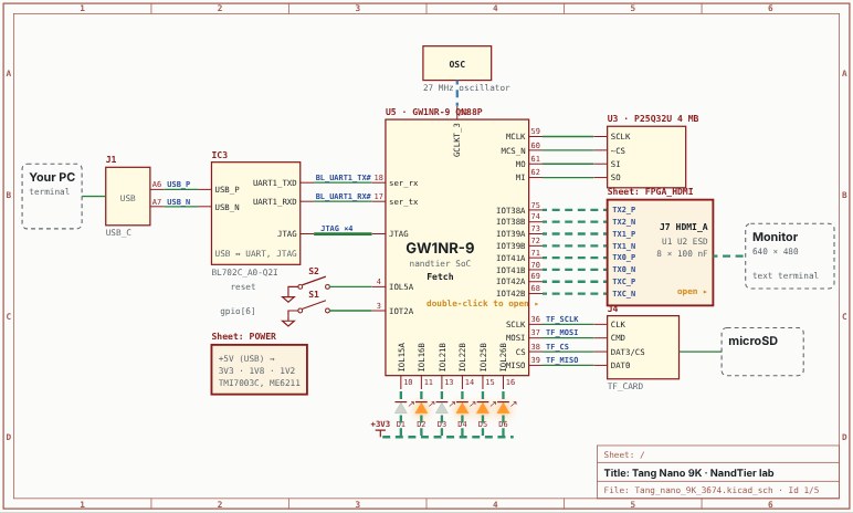
The Tang Nano 9K already has the wiring for it. The BL702 chip next to the USB connector shows up on the PC as a serial port, and two of its pins go to the FPGA: one carries bytes from the FPGA to the PC (ser_tx, pin 17), the other from the PC to the FPGA (ser_rx, pin 18). What is missing is the logic in the FPGA that turns a byte into pulses on that wire, and pulses back into a byte. That logic is a UART.
How a byte travels on one wire
A UART line is idle high. To send a byte, the sender pulls the line low for one bit time (the start bit), then sends the 8 data bits, least significant first, then holds the line high for one bit time (the stop bit). Ten bit times per byte.
Both ends agree on the bit time in advance. At 115200 baud a bit lasts 1/115200 s, about 8.68 µs. Our clock runs at 24.975 MHz, so one bit is 24,975,000 / 115,200 ≈ 217 clock cycles. That number will appear everywhere in this article.
| Bit time | 1 | 8 data bits | 1 |
|---|---|---|---|
| Level | 0 (start) | b0 b1 … b7 | 1 (stop) |
A (0x41) on the line. Low for the start bit, then the bits from b0 to b7, then high for the stop bit. Each bit lasts 217 clock cycles.The module's ports
Everything in NandTier talks to the CPU the same way: a valid signal says an access is happening, addr, wdata and wstrb (which bytes are written) describe it, and the device answers with ready and rdata. We will look at that bus properly in the next article. For now, here is the UART's outside:
21module nt_uart #(22 parameter [15:0] DEFAULT_DIV = 16'd217, // 115200 baud at 25 MHz23 parameter FIFO_BITS = 4 // receive FIFO: 2^FIFO_BITS bytes24) (25 input clk,26 input resetn,27 28 input valid,29 input [31:0] addr,30 input [31:0] wdata,31 input [ 3:0] wstrb,32 output ready,33 output [31:0] rdata,34 35 input rx,36 output reg tx37);Two parameters: DEFAULT_DIV, the 217 from above, and FIFO_BITS, the size of a receive buffer we will add at the end. Besides the bus there are just two pins, rx and tx.
The register map is in the header comment of the file, and it is small: a write to offset 0 sends a byte, a read from offset 0 returns a received byte, and offset 4 holds the bit period.
9// Registers:10// +0x0 DATA read: oldest received byte in bits 7:0 (and removes it),11// or 0xFFFF_FFFF when nothing has been received12// write: send bits 7:0; the bus access waits while the13// previous byte is still being sent14// +0x4 DIV bit period in clock cycles, 16 bits (minimum 4)The transmitter
To send we need three things: the ten bits to shift out, how many are left, and a counter for the 217 cycles of the current bit.
45reg [ 9:0] tx_shift; // stop bit, 8 data bits, start bit (sent LSB first)46reg [ 3:0] tx_bits; // bits left to send, 0 = idle47reg [15:0] tx_count;48 49wire tx_busy = tx_bits != 4'd0;50wire tx_write = valid && !sel_div && wstrb[0];tx_shift holds the whole frame at once. tx_busy is true while bits are left. tx_write is a CPU write to the data register: offset 0 (!sel_div) with the lowest byte strobe set.
When such a write comes in and we are not busy, the frame is built in one step:
56end else if (tx_write && !tx_busy) begin57 tx_shift <= {1'b1, wdata[7:0], 1'b0};58 tx_bits <= 4'd10;59 tx_count <= 16'd0;{1'b1, wdata[7:0], 1'b0} is the stop bit, the data byte and the start bit, concatenated. Because we shift right and send bit 0 first, the start bit (0) goes out first and the stop bit (1) last, exactly the order on the wire. Ten bits to go, counter at zero.
While busy, every clock either counts or moves on to the next bit:
60end else if (tx_busy) begin61 tx <= tx_shift[0];62 if (tx_count == div - 16'd1) begin63 tx_count <= 16'd0;64 tx_shift <= {1'b1, tx_shift[9:1]};65 tx_bits <= tx_bits - 4'd1;66 end else begin67 tx_count <= tx_count + 16'd1;68 endtx always shows bit 0 of the shift register. When the counter reaches div - 1, the bit has lasted 217 cycles: shift right (filling with 1, the idle level), count one bit fewer, start the counter again. After ten bits tx_busy falls and the line goes back to idle high.
The receiver
Receiving is the same story backwards, with one catch: the rx pin is driven by another chip on its own clock. Its edges can arrive at any moment relative to our clock, and a flip-flop that samples a signal exactly as it changes can go metastable. So the pin first goes through a small synchroniser:
76reg [ 2:0] rx_sync; // synchroniser and edge detector77reg [ 3:0] rx_bits; // 0 = idle, else bits left including the stop bit78reg [15:0] rx_count;79reg [ 7:0] rx_shift;80reg rx_push;81 82wire rx_in = rx_sync[1];83 84always @(posedge clk) begin85 rx_sync <= {rx_sync[1:0], rx};rx_sync shifts the pin in every cycle. rx_in = rx_sync[1] has been through two flip-flops and is safe to use. rx_sync[2] is the value one cycle older, so rx_sync[2] && !rx_in means "the line just went from 1 to 0": a falling edge, the beginning of a start bit.
Now the key idea. We want to sample each bit in its middle, where it is stable, not at its edges. So when the start bit begins we wait half a bit, and from there whole bits:
91end else if (rx_bits == 4'd0) begin92 // start bit: wait half a bit period, then sample in the middle93 if (rx_sync[2] && !rx_in) begin94 rx_bits <= 4'd10;95 rx_count <= {1'b0, div[15:1]};96 end{1'b0, div[15:1]} is div / 2, 108 cycles. Ten "bits" to go: the start bit itself, eight data bits and the stop bit.
Each time the counter runs out we are in the middle of a bit, and what we do depends on which bit it is:
97end else if (rx_count != 16'd0) begin98 rx_count <= rx_count - 16'd1;99end else begin100 rx_count <= div - 16'd1;101 rx_bits <= rx_bits - 4'd1;102 case (rx_bits)103 4'd10: if (rx_in) rx_bits <= 4'd0; // glitch, not a start bit104 4'd1: rx_push <= rx_in; // keep it only with a valid stop bit105 default: rx_shift <= {rx_in, rx_shift[7:1]};106 endcase- In the middle of the start bit (
rx_bits == 10) the line must still be low. If it is high, the falling edge was a glitch, and we go back to idle. - For the data bits we shift the line into
rx_shiftfrom the top, so after eight bits the first one has arrived at bit 0, LSB first as sent. - In the middle of the stop bit the line must be high. Only then do we push the byte; a missing stop bit means a broken frame, and we drop it.
nt_uart, clock by clock (the bit period is shortened to 8 cycles so you can watch it). Send a character, or play the PC and send one back.A small receive buffer
If the CPU is busy drawing a frame when a key arrives, the next byte could overwrite the last. A 16-byte FIFO gives the software about 16 byte times, 35,000 cycles, of slack:
112reg [7:0] fifo [0:(1 << FIFO_BITS) - 1];113reg [FIFO_BITS:0] fifo_head, fifo_tail; // one extra bit tells full from empty114 115wire fifo_empty = fifo_head == fifo_tail;116wire fifo_full = fifo_head == {~fifo_tail[FIFO_BITS], fifo_tail[FIFO_BITS-1:0]};117wire rx_pop = valid && !sel_div && !is_write && !fifo_empty;The trick on line 113: head and tail pointers have one bit more than needed to address 16 entries. When they are equal the FIFO is empty; when only that extra bit differs, it is full.
The bus side
Finally the registers. The bit period can be changed by software:
135always @(posedge clk) begin136 if (!resetn)137 div <= DEFAULT_DIV;138 else if (valid && sel_div) begin139 if (wstrb[0]) div[ 7:0] <= wdata[ 7:0];140 if (wstrb[1]) div[15:8] <= wdata[15:8];141 end142endAnd the two lines that answer the CPU:
144assign ready = valid && !(tx_write && tx_busy);145assign rdata = sel_div ? {16'd0, div} :146 fifo_empty ? 32'hFFFF_FFFF :147 {24'd0, fifo[fifo_tail[FIFO_BITS-1:0]]};ready is the bus handshake: always immediate, except for a data write while the transmitter is busy, which waits. A read of the data register returns the oldest byte of the FIFO, or 0xFFFF_FFFF if it is empty. That all-ones value cannot be a byte, so software can tell "no data" from "a byte that happens to be 0xFF".
Wiring it in
The UART sits in the SoC top level, hw/nandtier.v, on the peripheral bus at 0x8300_0000:
268nt_uart u_uart (269 .clk(clk_sys), .resetn(soc_resetn),270 .valid(per_valid[3]), .addr(cpu_addr), .wdata(cpu_wdata), .wstrb(cpu_wstrb),271 .ready(per_ready[3]), .rdata(uart_rdata),272 .rx(ser_rx), .tx(ser_tx)273);274 275// every byte written to the UART data register also goes to the screen276wire term_valid = per_valid[3] && per_ready[3] && !cpu_addr[2] && cpu_wstrb[0];The last two lines are a bonus: every byte the CPU writes to the UART is also handed to the HDMI text terminal (part 9), so the same text appears in the PC terminal and on the screen.
Using it from C
The firmware sees the UART as two memory locations. nandtier.h names them:
27#define NT_REG(addr) (*(volatile uint32_t *)(addr))28#define NT_REG8(addr) (*(volatile uint8_t *)(addr))29 30// --- UART ------------------------------------------------------------------------31 32#define UART_DATA NT_REG(NT_UART_BASE + 0x0) // read: byte or 0xFFFFFFFF if none33#define UART_DIV NT_REG(NT_UART_BASE + 0x4) // bit period in clock cyclesNT_REG turns an address into a volatile 32-bit variable; volatile tells the compiler that every read and write really has to happen, in order, because the value can change behind its back. With that, sending a character is one assignment:
7void print_char(char c)8{9 if (c == '\n')10 UART_DATA = '\r';11 UART_DATA = (uint8_t)c;12}The '\r' before every '\n' is for terminals, which need a carriage return to go back to the start of the line. Receiving is a loop on the "nothing yet" value:
38char get_char(void)39{40 uint32_t v;41 while ((v = UART_DATA) == 0xFFFFFFFFu)42 ;43 return (char)v;44}Note what is not there: no check that the transmitter is free. The hardware's ready makes the store wait, so UART_DATA = c just takes a little longer when the UART is busy.
Trying it
With the board programmed, open a terminal on its serial port. On Linux it is usually the second of the two ports the BL702 creates:
$ screen /dev/ttyUSB1 115200Press S1 on the board. The boot ROM waits half a second for a programmer, then starts the launcher, and its menu appears. Type B and the CPU runs a benchmark and prints its cycle count back to you, every character through the module above.
Conclusion
A UART is two shift registers and two counters, and with it the board can finally talk. Every later piece of the series, from the CPU's first instructions to the game launcher, reports back through this module.
So far though, "the CPU writes to 0x8300_0000" has been taken on faith. How does an address turn into a selected device? In the next article we build the bus and the memory map.