The Bus and the Memory Map
One set of wires from the CPU to every device, an address decoder that picks the right one, and our first peripheral the CPU can blink.
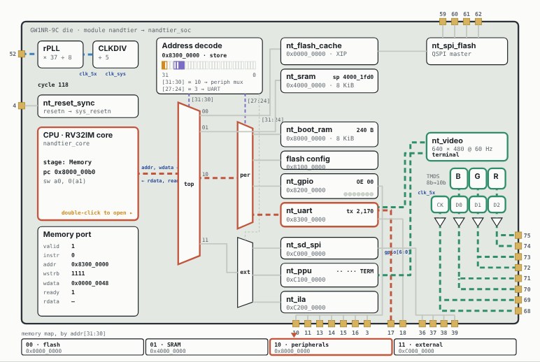
In this article
What are we trying to do?
Our computer will have one CPU and many things for it to talk to: two kinds of RAM, the flash, the UART, the LEDs, the SD card, the graphics chip. The CPU should not need a separate set of wires for each. Instead it gets one bus: an address, data in each direction, and a few control signals, and every device sits somewhere on a single map of addresses.
So we need two things: a protocol that every device speaks, and a decoder that looks at an address and decides which device it belongs to.
The protocol: valid and ready
NandTier uses a simple handshake. The CPU sets the address, raises valid, and (for a write) puts the data on wdata with wstrb saying which of the four bytes to write. The device answers by raising ready, with the read data on rdata. The access is over in the cycle where both are high.
| Signal | From | Meaning |
|---|---|---|
valid | CPU | an access is happening |
addr | CPU | byte address, 32 bits |
wdata | CPU | data to write |
wstrb | CPU | one bit per byte to write; 0000 means a read |
ready | device | done (this cycle) |
rdata | device | the data read |
The nice thing about ready is that a device decides its own speed. The UART answers in the same cycle; the flash may take hundreds of cycles to fetch a line; the CPU simply waits. We already used that in part 2, where a UART write waits for the transmitter.
valid, ready and the data move.The memory map
Here is where everything lives, straight from the top of hw/nandtier.v:
11// Memory map:12// 0x0000_0000 SPI flash, execute in place (16 MiB window), from flash13// address FLASH_OFFSET on (0 on the Tang Nano 9K, whose14// bitstream lives inside the FPGA; other boards keep the15// bitstream at the start of the same flash)16// 0x4000_0000 SRAM, 8 KiB17// 0x8000_0000 boot RAM, 8 KiB (boot ROM image, reset vector)18// 0x8100_0000 SPI flash config / bit-bang register19// 0x8200_0000 GPIO20// 0x8300_0000 UART (every byte sent also goes to the HDMI terminal)21// 0xC000_0000 SD card SPI port22// 0xC100_0000 picture processing unit (tiles, sprites; see hw/video/nt_ppu.v)23// 0xC200_0000 on-chip logic analyzer (CPU bus trace)Look at the top two bits of each address: 00 is the flash, 01 the SRAM, 10 the boot RAM and simple peripherals, 11 the SD card and the graphics. That is not an accident. The first decision only needs two bits, and then each quarter is split further. The reset vector, 0x8000_0000, is the first word of the boot RAM, so the CPU's very first instruction comes from there.
A decoder with four outputs
The whole bus is built from one small module, used three times: one master, four slaves, each slave given a base address and a mask.
16module nt_bus_mux4 #(17 parameter [31:0] BASE0 = 32'h0000_0000, MASK0 = 32'hC000_0000,18 parameter [31:0] BASE1 = 32'h4000_0000, MASK1 = 32'hC000_0000,19 parameter [31:0] BASE2 = 32'h8000_0000, MASK2 = 32'hC000_0000,20 parameter [31:0] BASE3 = 32'hC000_0000, MASK3 = 32'hC000_000021) (22 input m_valid,23 input [31:0] m_addr,24 output m_ready,25 output [31:0] m_rdata,26 27 output [ 3:0] s_valid, // bit n: slave n28 input [ 3:0] s_ready,29 input [31:0] s0_rdata,30 input [31:0] s1_rdata,31 input [31:0] s2_rdata,32 input [31:0] s3_rdata33);A slave matches when the address bits selected by its mask equal its base address:
34wire [3:0] hit = {(m_addr & MASK3) == (BASE3 & MASK3),35 (m_addr & MASK2) == (BASE2 & MASK2),36 (m_addr & MASK1) == (BASE1 & MASK1),37 (m_addr & MASK0) == (BASE0 & MASK0)};With MASK = 32'hC000_0000 only bits 31:30 are compared, so slave 1 with base 0x4000_0000 gets every address from 0x4000_0000 to 0x7FFF_FFFF.
If two slaves match, the lowest one wins. That uses a classic bit trick:
40wire [3:0] sel = hit & ~(hit - 4'd1);41 42assign s_valid = {4{m_valid}} & sel;hit - 1 flips the lowest set bit and every zero below it; & ~(...) keeps only that lowest set bit. So 0110 becomes 0010. s_valid is then valid routed to exactly one slave.
And the way back:
44assign m_ready = sel == 4'd0 ? m_valid : |(s_ready & sel);45 46assign m_rdata = ({32{sel[0]}} & s0_rdata) |47 ({32{sel[1]}} & s1_rdata) |48 ({32{sel[2]}} & s2_rdata) |49 ({32{sel[3]}} & s3_rdata);The CPU's ready is the selected slave's ready. If no slave matches, the access is acknowledged at once with data 0: a stray pointer reads zeros instead of hanging the CPU forever. The read data is an AND-OR multiplexer: each slave's data is masked by its select bit, and the results are ORed.
Building the tree
In the SoC top level the first decoder splits on bits 31:30:
171nt_bus_mux4 #(172 .BASE0(32'h0000_0000), .MASK0(32'hC000_0000),173 .BASE1(32'h4000_0000), .MASK1(32'hC000_0000),174 .BASE2(32'h8000_0000), .MASK2(32'hC000_0000),175 .BASE3(32'hC000_0000), .MASK3(32'hC000_0000)176) u_bus_top (177 .m_valid (cpu_valid),178 .m_addr (cpu_addr),179 .m_ready (cpu_ready),180 .m_rdata (cpu_rdata),181 .s_valid (top_valid),182 .s_ready (top_ready),183 .s0_rdata(flash_rdata),184 .s1_rdata(sram_rdata),185 .s2_rdata(periph_rdata),186 .s3_rdata(ext_rdata)187);The third quarter, 0x8000_0000, is the boot RAM plus three small peripherals, so a second decoder splits it on bits 27:24:
194nt_bus_mux4 #(195 .BASE0(32'h8000_0000), .MASK0(32'h0F00_0000),196 .BASE1(32'h8100_0000), .MASK1(32'h0F00_0000),197 .BASE2(32'h8200_0000), .MASK2(32'h0F00_0000),198 .BASE3(32'h8300_0000), .MASK3(32'h0F00_0000)199) u_bus_periph (200 .m_valid (top_valid[2]),201 .m_addr (cpu_addr),202 .m_ready (top_ready[2]),203 .m_rdata (periph_rdata),204 .s_valid (per_valid),205 .s_ready (per_ready),206 .s0_rdata(bootram_rdata),207 .s1_rdata(flashcfg_rdata),208 .s2_rdata(gpio_rdata),209 .s3_rdata(uart_rdata)210);Its input is the first decoder's slave 2: top_valid[2] and top_ready[2]. That makes a tree. A write to the UART at 0x8300_0000 matches slave 2 at the top, then slave 3 here.
A third decoder does the same for 0xC000_0000 (SD card, PPU, logic analyser). The devices themselves hang off the leaves, all sharing the CPU's address and write data, each with its own valid:
214nt_sram u_sram (215 .clk(clk_sys), .resetn(soc_resetn),216 .valid(top_valid[1]), .addr(cpu_addr), .wdata(cpu_wdata), .wstrb(cpu_wstrb),217 .ready(top_ready[1]), .rdata(sram_rdata)218);219 220nt_boot_ram u_boot_ram (221 .clk(clk_sys), .resetn(soc_resetn),222 .valid(per_valid[0]), .addr(cpu_addr), .wdata(cpu_wdata), .wstrb(cpu_wstrb),223 .ready(per_ready[0]), .rdata(bootram_rdata)224);Our first peripheral: GPIO
Now let us put a device on the bus that does something visible. The six LEDs and the S1 button are wired to FPGA pins as gpio[0..6]. A GPIO block gives the CPU three registers: OUT (the level to drive), IN (what the pins read) and OE (which pins are outputs).
34reg [31:0] out, oe;35reg [WIDTH-1:0] in_meta, in_sync;36 37function [31:0] merge(input [31:0] old, input [31:0] upd, input [3:0] strb);38 integer b;39 for (b = 0; b < 4; b = b + 1)40 merge[b*8 +: 8] = strb[b] ? upd[b*8 +: 8] : old[b*8 +: 8];41endfunctionmerge applies a write with byte strobes: for each of the four bytes, the new value if its strobe is set, the old one otherwise. A byte store to OUT changes just that byte. Every register in NandTier that can be written with byte stores uses the same pattern.
The bus side of GPIO takes one cycle to answer, so ready is a register:
43always @(posedge clk) begin44 in_meta <= io ^ INVERT;45 in_sync <= in_meta;46 ready <= 1'b0;47 48 if (!resetn) begin49 out <= 32'd0;50 oe <= 32'd0;51 end else if (valid && !ready) begin52 ready <= 1'b1;53 case (addr[3:2])54 2'd0: begin55 out <= merge(out, wdata, wstrb);56 rdata <= out;57 end58 2'd1: rdata <= {{(32-WIDTH){1'b0}}, in_sync};59 2'd2: begin60 oe <= merge(oe, wdata, wstrb);61 rdata <= oe;62 end63 default: rdata <= 32'd0;64 endcase65 end66endaddr[3:2] picks the register: word 0 OUT, word 1 IN, word 2 OE. The input pins go through two flip-flops (in_meta, in_sync) before the CPU sees them, the same synchroniser as the UART's receiver, because a button press is just as asynchronous as a serial line.
Finally the pins themselves:
68genvar n;69generate70 for (n = 0; n < WIDTH; n = n + 1) begin : pin71 assign io[n] = oe[n] ? out[n] ^ INVERT[n] : 1'bz;72 end73endgenerateA pin with its OE bit set drives OUT; otherwise it is 1'bz, high impedance, and can be read. INVERT exists for boards whose LEDs are wired the other way round.
OUT and OE, press the switches, read IN: the synchroniser delay shows up as two clocks.Blinking from C
With GPIO at 0x8200_0000 and the cycle counter from the CPU, a blinking LED is a few lines:
#include "nandtier.h" int main(void){ GPIO_OE = 0x3F; // pins 0..5 drive the LEDs for (uint32_t n = 0;; n++) { GPIO_OUT = ~n; // a binary counter, lit = 1 uint32_t t = nt_cycles(); while (nt_cycles() - t < NT_CLK_HZ / 8) ; // an eighth of a second }}~n because the LEDs are active low. nt_cycles() reads the CPU's cycle counter with the rdcycle instruction:
191static inline uint32_t nt_cycles(void)192{193 uint32_t c;194 __asm__ volatile ("rdcycle %0" : "=r"(c));195 return c;196}Conclusion
The bus is the backbone of the SoC: one handshake that every device speaks, and a 51-line decoder used three times to build the memory map. From here on, a new peripheral is just a module with valid, ready and a few registers, hung on a free slot.
Something still has to drive the bus, though. In the next two articles we build the thing that issues all those addresses: the RISC-V CPU.