Installation & Getting Started
What we are building, the open-source toolchain that turns Verilog into a bitstream, and the first time the board lights up.
In this article
What are we trying to do?
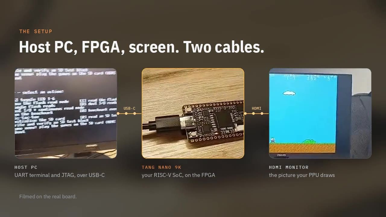
Start with the end. On the desk there is a Tang Nano 9K, a monitor and a USB cable. When it is finished, the board boots, prints a menu over the serial port, and plays games on the HDMI screen. Nothing on the board does that today: the FPGA on it is a blank sheet of logic, and every part of that computer has to be described by us.
So this series has two kinds of text in it. Verilog describes the hardware: the processor, the bus, the serial port, the video output. C is the software that runs on that hardware: the boot ROM, the launcher, the games. The goal is simple to say: make the board become the computer, then make it run the C.
Between the text and the board sits a chain of tools. In this first article we install them, find our way around the project, and build the whole thing once, so that every later article can change one piece and see it run.
The Tang Nano 9K
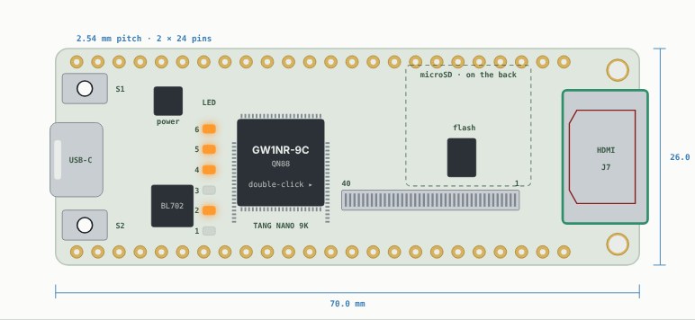
The board is built around a Gowin GW1NR-9C FPGA: about 8,640 lookup tables, a block of on-chip RAM, a PLL to make clocks, and pins that can be wired to almost anything. Around it Sipeed put the things we will use:
- a 27 MHz crystal, the only clock on the board
- a USB-C port with a BL702 chip that gives the PC a serial port to the FPGA
- an HDMI connector wired straight to FPGA pins
- a microSD slot and a 4 MiB SPI flash chip
- six LEDs and two buttons
The programming process
An FPGA is programmed with a bitstream: a file that sets every lookup table, flip-flop and routing switch on the chip. Getting from Verilog to that file takes three steps, and it helps to know what each one does before we run them.
Synthesis
Synthesis reads the Verilog and turns it into a netlist of the cells this FPGA actually has: 4-input lookup tables (LUT4), flip-flops (DFF), carry chains (ALU), block RAMs. An assign y = a & b; becomes one LUT whose truth table is AND. A 32-bit adder becomes a chain of 32 ALU cells. The tool is Yosys.
synth_gowin. Click a cell to see what it is.Place and route
The netlist says what cells we need and how they connect, but not where. Place and route picks a physical cell on the chip for each one (placing), then finds wires through the switch matrix to connect them (routing), and checks that signals arrive in time for the clock. The tool is nextpnr, in its himbaechel flavour for Gowin chips.
Bitstream generation
Finally the placed and routed design is packed into the bits the chip loads. For Gowin chips the open-source tool is gowin_pack, from project Apicula, which reverse-engineered the format. Then openFPGALoader sends the file over USB.
The open-source toolchain
All of these tools come together in the YosysHQ OSS CAD Suite: one download with Yosys, nextpnr, Apicula, openFPGALoader and Icarus Verilog for simulation. For the C side we also need a RISC-V cross compiler, the xPack riscv-none-elf-gcc, and Python with pyserial for the PC tools.
You do not have to collect them by hand. The repository has a setup script that downloads every tool, at the versions the course was tested with, into a tools/ folder inside the project. Nothing is installed system-wide, so deleting that folder removes it all again.
$ setup/setup.sh # Linux, macOS, WSL$ setup\setup.bat # Windows: double-click, or run in a terminalIt unpacks the archives, checks every tool, and finishes by building the firmware once:
==> checking ok riscv-none-elf-gcc (xPack GNU RISC-V Embedded GCC x86_64) 14.2.0 ok yosys: Yosys 0.70+286 ok nextpnr-himbaechel: nextpnr-0.11.1 ok openFPGALoader: openFPGALoader v1.2.0 ok iverilog: Icarus Verilog version 14.0 (devel) ok Python 3.13.18 with pyserial==> building the boot ROM, the launcher and the games (make) ok firmware built: fw/fw-flash/build/fw-flash.v, fw/games/build/carts.imgHow do the Makefiles find the tools? The script writes them into local.mk at the top of the repository, and every Makefile reads that file first. In the FPGA Makefile:
36NT_HERE := $(dir $(lastword $(MAKEFILE_LIST)))37# Tool locations written by setup/setup.sh or setup/setup.ps1 (see README,38# "Setting up"); a variable given on the command line or in the environment wins.39-include $(NT_HERE)../local.mk40OSS_CAD ?= $(abspath $(NT_HERE)../tools/oss-cad-suite)41BIN = $(if $(OSS_CAD),$(OSS_CAD)/bin/)42 43YOSYS = $(BIN)yosys44LOADER = $(BIN)openFPGALoader-include reads local.mk if it is there (the - means "no error if not"). Every setting in it uses ?=, so a value you give on the command line, make OSS_CAD=/opt/oss-cad-suite, still wins. BIN becomes the suite's bin/ folder; set OSS_CAD= (empty) and the tools are found on your PATH instead.
The compiler is found the same way:
22CC = $(RISCV_PATH)/bin/$(RISCV_NAME)-gcc23OBJCOPY = $(RISCV_PATH)/bin/$(RISCV_NAME)-objcopy24OBJDUMP = $(RISCV_PATH)/bin/$(RISCV_NAME)-objdump25 26# The core is RV32I only: no M (mul/div) and no C (compressed) extension.27# GCC 12 and later want the CSR instructions (rdcycle) named as Zicsr; older28# compilers (riscv-none-embed 8.x) do not know the name, so ask the compiler.29ZICSR := $(shell $(CC) -march=rv32i_zicsr -mabi=ilp32 -E -x c /dev/null >/dev/null 2>&1 && echo _zicsr)30ARCH = -march=rv32i$(ZICSR) -mabi=ilp3231OPT ?= -O2RISCV_PATH and RISCV_NAME choose the compiler; any bare-metal riscv32/riscv64 GCC works if you point them at it. Two comments are worth noticing already. The firmware is compiled for plain RV32I, the base integer instruction set, which we will build in parts 4 and 5. And newer GCCs want the instructions that read counters (rdcycle) named as the Zicsr extension, so the Makefile asks the compiler once whether it knows that name.
The project
Clone the NandTier repository and look around. Every folder is one layer of the machine:
| Folder | What is in it |
|---|---|
hw/ | The SoC in Verilog: core/ (the CPU), bus/, mem/, periph/, video/ |
boards/ | Per-board top levels, pin constraints and clocks |
oss/ | The open-source FPGA build (the Makefile above) |
fw/ | The C: fw-brom/ (boot ROM), fw-flash/ (launcher), games/, sdk/ |
sw/ | PC tools: the programmer, the SD pack builder, the gamepad bridge |
test/, sim/ | Testbenches for every module, and a whole-SoC simulation |
Telling the tools about the board
The Verilog says the top module has ports called clk, ser_tx, tmds_d_p and so on. Nothing yet says which pin of the chip each one is. That is the job of the constraints file, .cst for Gowin:
7// 27 MHz crystal, S1 button8IO_LOC "clk" 52;9IO_PORT "clk" IO_TYPE=LVCMOS33 PULL_MODE=UP;10IO_LOC "resetn" 4;11IO_PORT "resetn" PULL_MODE=UP;IO_LOC ties a port to a pin number: clk to pin 52, where the crystal is, and resetn to pin 4, the S1 button. IO_PORT sets the electrical side: 3.3 V CMOS levels and a pull-up, so the button reads 1 when nobody presses it.
The serial port is two more lines, the pins that go to the USB bridge:
27// UART through the on-board BL702 (USB)28IO_LOC "ser_tx" 17;29IO_PORT "ser_tx" IO_TYPE=LVCMOS33 PULL_MODE=UP DRIVE=8;30IO_LOC "ser_rx" 18;And the board file collects everything nextpnr and gowin_pack need to know about the board in one place:
8BOARD_NAME = Sipeed Tang Nano 9K9VENDOR = gowin10TOP = nandtier11BOARD_SRC = boards/tangnano9k/gowin_ip.v boards/common/nt_rams.v12 13DEVICE = GW1NR-LV9QN88PC6/I514FAMILY = GW1N-9C15SYNTH_FLAGS =16CST = boards/tangnano9k/tangnano9k.cst17SDC = boards/tangnano9k/tangnano9k.sdc18PACK_FLAGS = --mspi_as_gpio19 20LOADER_BOARD = tangnano9k21FLASH_OFFSET = 0x000000DEVICE is the exact chip, including package and speed grade; FAMILY is what gowin_pack calls it. PACK_FLAGS = --mspi_as_gpio is a small but important line: the flash pins double as the FPGA's configuration pins, and this flag lets our design use them as normal I/O once the FPGA has started.
Running the build
Now the three steps from above, as the Makefile runs them. Synthesis first:
84$(OUT)/nandtier.json: $(SRC) $(BROM) | $(OUT)85 cp $(BROM) $(OUT)/86 cd $(OUT) && $(YOSYS) -q -l yosys.log -p "read_verilog $(DEFINES) $(addprefix ../../,$(SRC)); \87 $(SYNTH); techmap t:\$$buf; opt_clean -purge; \88 write_json nandtier.json; tee -o stat.txt stat"read_verilog reads every file in hw/ plus the board's; synth_gowin -top nandtier does the synthesis; write_json saves the netlist for the next tool, and stat writes a cell count to stat.txt. The boot ROM's .hex files are copied next to it first, because the boot RAM is filled with them at synthesis (part 6).
Then place and route:
92$(OUT)/nandtier_pnr.json: $(OUT)/nandtier.json $(ROOT)/$(CST) $(ROOT)/$(SDC)93 $(BIN)nextpnr-himbaechel --json $< --write $@ --device $(DEVICE) --vopt family=$(FAMILY) \94 --vopt cst=$(ROOT)/$(CST) --sdc $(ROOT)/$(SDC) --report $(OUT)/report.json \95 -l $(OUT)/nextpnr.log -q96 @grep -E "Max frequency for clock" $(OUT)/nextpnr.log | tail -3The constraints come in through --vopt cst= and the timing goal through the .sdc file. After routing, the Makefile prints the line from the log that matters most: the maximum frequency each clock can run at. If that number is below the clock we run, the design will misbehave on the board.
And the bitstream:
99$(OUT)/nandtier.fs: $(OUT)/nandtier_pnr.json100 $(BIN)gowin_pack -d $(FAMILY) $(PACK_FLAGS) -o $@ $< 2> $(OUT)/gowin_pack.log || \101 { cat $(OUT)/gowin_pack.log; exit 1; }102 @echo "Bitstream for the $(BOARD_NAME): oss/$@"Run it all with one command from the top of the repository. The first build also compiles the boot ROM, because the bitstream contains it:
$ make fpgaWhen it finishes you get oss/build/tangnano9k/nandtier.fs. Load it into the FPGA:
$ make fpga-loadfpga-load writes the FPGA's SRAM, so the design is gone at power-off; that is what you want while developing. make fpga-flash writes the FPGA's own configuration flash, and the board starts the design by itself from then on.
The firmware
The bitstream is only half the machine. The rest is software, built by the top-level Makefile:
$ make # boot ROM, launcher and the game cartridges$ make program COMx=/dev/ttyUSB1make program sends the launcher into the SPI flash and the games onto the SD card, through the boot ROM, over the serial port. Open a terminal on the board's serial port at 115200 baud, press S1 to reset, and the launcher's menu appears, both in the terminal and on the HDMI screen.
Conclusion
We now have the tools, a map of the project, and a board that runs the finished NandTier. That is the end point; the rest of the series walks back to the start and builds it up one piece at a time, so that every line in it is something you have seen and understood.
The first piece is the one that lets the board talk back: in the next article we build the UART, the serial port, from a shift register and a counter.